 |
|
 |
| |

Dear Readers,
This is the fourth of a series of reviews on selected topics of electrical/electronic connector
technology. You are invited to suggest a review topic of interest.
R.S. Timsit
Timron Advanced Connection Technologies, A Division of Timron Scientific Consulting Inc., Toronto, Ontario, Canada M5M 1L6
Tel: 416-787-8161,
www.timron-inc.com
|
 |

ELECTRICAL CONTACT RESISTANCE: REVIEW OF ELEMENTARY CONCEPTS
The service life of bulk electrical interconnections such as in electrical sockets, switches or other connection devices,
is affected by factors such as residual contact force, vibrations, corrosion etc.. These factors generally succeed in
compromising the integrity of contact interfaces and lead to the eventual degradation and failure of all electrical connections.
The time to failure depends on the connection technology and on the connector service environment, and varies widely from hours
to tens of years. Failure is always preceded by a significant increase in contact resistance at the electrical interfaces.
As we will see, contact resistance originates from the fundamental property of electrical junctions that the area of metallic
contact is generally very small. Degradation stems from a large decrease in this small area of contact due to the synergistic
action of failure-inducing mechanisms.
Fundamental Properties of Electrical Contacts
Electrical contact resistance in bulk electronic connections stems from the presence of roughness on the mating surfaces.
Contact between two surfaces occurs at discrete spots determined by the distribution of roughness asperities on the two surfaces, as
illustrated in Fig. 1(a). These contact spots are also known as “a-spots”. For all solid materials the area of true contact is
thus a small fraction (often only a fraction of 1%) of the nominal contact area, even at contact loads of tens of kilograms [1-3].
Such a contact area is illustrated schematically in Fig. 1(b). In a bulk electrical junction, the electrical current lines bundle
together to pass through a-spots, also as illustrated in Fig. 1(a). Constriction of the electrical current at an electrical interface
gives rise to an electrical “contact resistance” in the same way as resistance to water flow in a hose is increased by constricting
the hose. In a practical electrical connection, the total area of electrical contact must be made as large as practicable to minimize
contact resistance. In contrast, loss of true contact area leads to contact degradation.
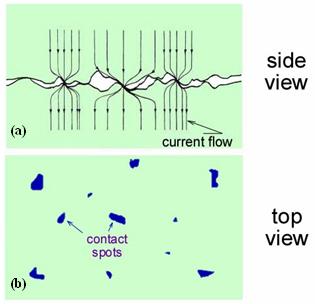
Fig. 1.(a) Schematic diagram of a bulk electrical interface
(b) spots in blue indicate spots of true contact.
Because the true area of contact is much smaller than the apparent contact area, a-spots must support local mechanical pressures
that are larger than the yield strength of the materials in contact [2,3]. The consequence is that contacting asperities deform permanently
according to their mechanical hardness. It turns out that this deformation mode of contacting asperities allows an evaluation of contact
resistance in terms of hardness and contact force. For monometallic contact surfaces that are free of insulating contaminants, the contact
resistance is given as [1-3]
Rc = {ρ2πH / 4F}1/2
where ρ is the electrical resistivity of the contacting materials, H is the Vickers’ hardness of the softer of the contact surfaces and
F is the contact force. The variation of contact resistance with mechanical contact load as evaluated from the above expression is
illustrated in Fig. 2 for copper.
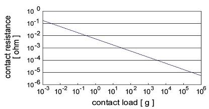
Fig. 2. Contact resistance versus contact load for a copper contact.
Note that the contact resistance decrease rapidly to the milliohm range for contact loads of a few hundred grams i.e. the load range
encountered in many electronic contact devices.
The relative simplicity of the expression for Rc masks the complexity of the physical phenomena involved in the generation of an electrical interface.
The variation in contact resistance with contact load depicted in Fig. 2 stems from a combination of several factors: (1) an increase in the
number of contacting surface asperities as the nominal surfaces are brought closer together under the influence of an increasing load, (2)
permanent flattening of the contacting asperities, which reduces the constriction resistance associated with
each contact spot and thus reduces the overall contact resistance, and (3) work-hardening of the deformed contact asperities, which reduces the
rate of asperity flattening etc. The last effect decreases the rate at which contacting asperities flatten and thus reduces the rate at which new
asperities are brought into play as the load is increased further.
Upon passage of an electrical current, the temperature of an electrical contact spot rises to a near-equilibrium value in a short time, usually in
less than 1 microsecond [1,2]. Because
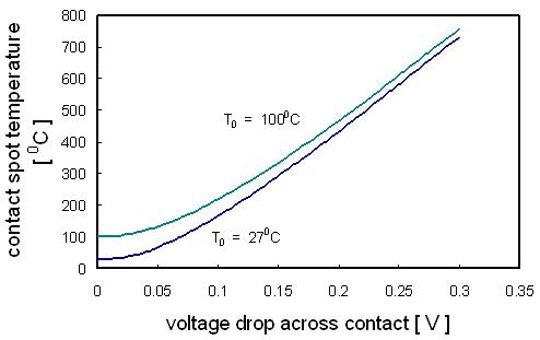
Fig. 3. Variation of contact spot temperature with voltage drop across a contact interface,
for connections with a bulk temperature respectively of 27°C and 100°C.
contact spots are small, very little heat produced within a contact spot is lost by convection to the (e.g. the air). Most of the heat is dissipated by conduction
through the surfaces in contact. This unique effect leads to an important relation between the maximum temperature Tm in a contact spot and the voltage V
across the contact as (V-T relation)
V2 = 4L (Tm2 – T02)
where L is the Lorenz constant (2.45 x 10⁻⁸ V2 / K2), T0 is the bulk temperature of the contact (i.e. far from contact spots)
and Tm and T0 are expressed in
Kelvin (K). The above V-T relation is independent of the materials in contact. The reasons for this interesting relation between voltage and contact spot
temperature are discussed in detail in other references [1,2], but they stem from an interrelation between the electrical resistivity and thermal conductivity
of metals through the Lorenz constant. Figure 3 shows the variation of the contact spot temperature Tm with increasing voltage across the contact
as evaluated from the V-T relation. The curves apply to all metal combinations. Note that the generation of a voltage as small as 0.1 V is sufficient to
heat contact spots to a temperature in excess of 150°C even where the bulk temperature of a contact is only 27°C. A tin-tin contact spot melts at a voltage
drop of 0.13 V (corresponding to the melting point of tin at 232°C). The data of Fig. 3 indicates that a voltage drop across a contact may be associated with
the melting point of contact spots in any monometallic interface. In the electrical contact literature, this parameter is known as the “melting voltage” and is
listed in Table 1 for a few commonly used contact materials.
Table 1
Voltage for Melting (Vm) of Common Electrical Contact Materials
| Material |
Vm (V) |
| Ni |
0.16 |
| Cu |
0.43 |
| Zn |
0.17 |
| Ag |
0.37 |
| Sn |
0.13 |
| Au |
0.43 |
| Pd |
0.57 |
The data of Fig. 3 are important in connector design for several reasons. First they indicate that the important parameter in determining contact spot temperature is
the voltage drop across the contact, not the current. Of course, the magnitude of the electrical current cannot be ignored since a large current may heat up the body
of a connector i.e. electrical current affects the value of T0 in Fig. 3. But it is the voltage drop across the contact caused by this current that bears a direct
relation to the contact spot temperature. The data of Fig. 3 and Table 1 also indicate that a connector must be designed so that the voltage drop across contact
interfaces must be significantly smaller than 0.1 V (and should generally not exceed about 0.010 V) under the largest current surge if contact spots are to remain cool
and thermally stable.
Contact Degradation
As mentioned earlier, degradation of electrical contacts stems from the loss of a-spots. This loss may be caused by a number of mechanisms such as oxidation,
galvanic corrosion, mechanical vibrations, fretting wear, and other mechanisms. It is important to emphasize that the expression for Rc given
above is valid only if the mating surfaces are free of electrically-insulating surface films, such as oxide or other corrosion films.
Any insulating surface films must be fractured, as illustrated in Fig. 4, to allow metallic conduction. Generally, the dimensions of cracks in the
insulating film depend on the thickness of the film and may be so small as to yield a very large contact resistance. This increase in
contact resistance is illustrated in Fig. 5 which shows the effect of oxide or other galvanic-corrosion films on nickel, copper and silver. Note
that a contaminant layer with a thickness of only a few nanometers on nickel or copper, leads to a large increase in contact resistance. Contaminant
films on silver consist largely of silver sulfide tarnish. These contaminant layers fracture relatively easily and do not adhere well to the underlying
metal. For these reasons, silver sulfide layers on silver are easier to disrupt and are deleterious to contact resistance only where the thickness is relatively large.
Contaminant films may also form by galvanic corrosion of the materials in contact. One of the well-known corrosion mechanisms is pore corrosion in gold-plated
surfaces. As suggested by its name, this type of corrosion stems from the presence of tiny pores (usually sub-micron in dimensions) in the gold
electroplate used as a finish on many connector surfaces. These pores allow access of corrosive environmental contaminants such as hydrogen sulfide, sulfur dioxide
and chlorides, along with moisture, to the nickel underplate or other substrate materials. Synergistic chemical reactions of the contact materials with the
contaminants and water lead to the formation of solid corrosion products that creep out of the pores and spread along the contact surfaces. Examples of
these corrosion “blooms” are shown in Fig. 6 [4]. A striking example of the formation of copper sulfide corrosion products generated below a gold electroplate
is shown in the cross-section of Fig. 7 [5]. Pore corrosion blooms of the type illustrated in Fig. 6 give rise to increases in contact resistance of the
magnitude illustrated in Fig. 5, and cause severe contact degradation.
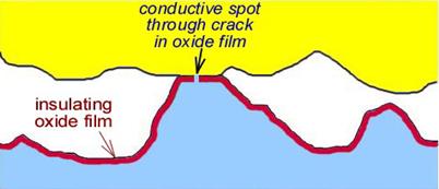
Fig.4. Schematic view of a contact spot with one surface covered
with a thin electrically-insulating layer.
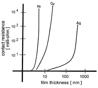
Fig. 5. Effect on contact resistance of the growth of oxide
and other galvanic-corrosion layers on nickel, copper
and silver surfaces.
The contact resistance was measured
with a gold probe pressed on the respective surfaces
after
exposure to a N2-O2-SO2-S8-H2O mixture at 30°C.
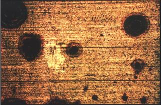
Fig. 6. Pore corrosion “blooms” generated through pores in a gold
electroplate on a copper surface exposed to a harsh environment [4].
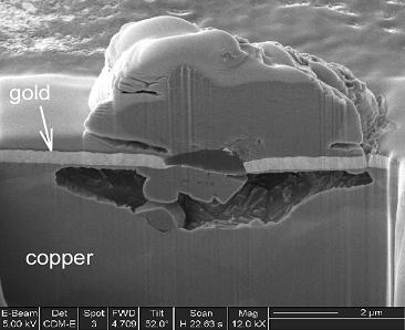
Fig. 7. Example of copper sulfidation through a pore in a gold layer [5].
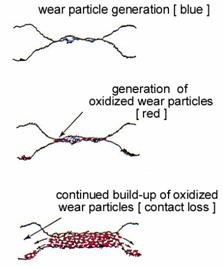
Fig. 8. Schematic representation of fretting wear.
Mechanical vibrations are generally deleterious to the stability of electrical contacts since they are conducive to a-spot disruption. The
severity of the impact of vibrations depends on several factors such as the type of surface finish, surface roughness, mechanical contact load and
other factors. Obviously, a sufficiently large contact load reduces the probability of a-spot shear-off.
The effects of differential thermal expansion on contact resistance between two contact surfaces are similar to those of mechanical vibrations.
One particularly worrisome effect of small-amplitude movement on contact resistance is fretting wear. This wear mechanism applies
specifically to interfaces where at least one of the surfaces oxidizes. As illustrated in Fig. 8, fretting wear leads to the formation of small
debris particles at the mechanical interface. In electronic connectors, the amplitude of this micromotion ranges from a few µm to about 100 µm.
Micromotion may be caused by external vibrations or by changing temperature due to differences in thermal expansion coefficients of the mating materials.
Oxidation of fretting debris leads to increased electrical contact resistance and eventually to complete electrical failure.
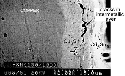
Fig. 9. Example of formation of Cu3Sn and Cu6Sn5 intermetallic
compounds at a tin-copper interface [6].
One mechanism that contributes often to electrical contact degeneration is intermetallics formation, particularly at interfaces between a plated
layer and the substrate material. Intermetallic compounds form as a result of interdiffusion between the two materials. The main deleterious effects
of intermetallics are a susceptibility to brittle fracture that leads to contact loss, as illustrated in Fig. 9 [6], and their relatively large
electrical resistivity compared with conventional contact materials large electrical resistivity enhances Joule heating of a-spots and thus promotes
contact degeneration.
One last major cause of connector degeneration we will consider is stress relaxation, which leads to loss of contact force. Stress relaxation describes
the reaction of the material in a mechanically-stressed connector component (e.g. a spring cantilever beam) to the load that generates this stress.
This reaction relieves the applied stress and thus reduces the mechanical load applied through that component. In the example of a simple cantilever
beam in a connector socket, the maximum stress located at the “anchored” end of the beam is slowly reduced by micro-flow and local redistribution of
material in the highly stressed region. The localized redistribution of material leads to a slight change in the local shape and subsequently to a slight
opening (offset) of the beam and an ensuing loss of contact load. A decrease in contact load leads to a loss of true contact area and increases in
contact resistance. The rate of stress relaxation generally depends on the composition and metallurgical state of the stressed material [4]. The rate
of stress relaxation increases rapidly with temperature. A loss of contact load obviously renders a contact more vulnerable to fretting wear and
to other deleterious effects of mechanical vibrations and differential thermal expansion.
Usually contact degradation mechanisms act synergistically to increase the rate of connector degeneration. This illustrated schematically in the flow diagram of Fig. 10.
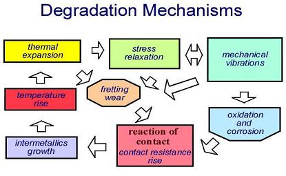
Fig. 10. Schematic representation of the synergistic action of
degradation mechanisms on electrical contacts.
References
- Holm, R., Electric Contacts, Theory and Applications, (Springer Verlag, Berlin, 1976).
- Timsit, R.S., "Electrical Contact Resistance: Fundamental Principles", in Electric Contacts: Theory and Applications, Ed. P.G. Slade, Marcel Dekker, Inc., New York, 1999.
- Timsit, R.S., Intensive Course on Electrical Contacts and Connector Design for Electronics and Microelectronics Applications, organized by Timron Advanced Connector Technologies, Toronto, ON, Canada; see details at www.timron-inc.com.
- Mroczkowski, R.S., Electronic Connector Handbook, McGraw-Hill, New York, 1998.
- Sun, A.C., Moffat, H.K., Enos, D.G. and Glauner, C.S., “Pore Corrosion Model for Gold-Plated Copper Contacts, Proc. 51st IEEE Holm Conference on Electrical Contacts, Chicago, IL, p. 232, 2005.
- Braunovic, M., "Effect of Intermetallic Phases on the Performance of Tin-Plated Copper Connections and Conductors”, Proc. 49st IEEE Holm Conference on Electrical Contacts, Washington, DC, p. 124, 2003.
|
 |
|
 |
|
 |
|